Meta harness makes 10 times better Kimi K3 chip
Several amazing friends texted me after seeing Kimi K3's autonomous chip design demo in their technical blog.1 It's super creative to demo the recursive setup of "model designs its own chip to run itself." Although it is not a commercial setup, it reveals that LLMs can, in a certain setup, go through the full RTL-to-GDS flow end to end. It's quite a precursor of something bigger happening beyond the software development space.
Reminder: similar to the Kimi blog post, the chip serves a ~1M-parameter "nano model," not the full 2.8T-parameter K3. We can apply similar harness on full size model, but here the goal is to exemplify a setup that allows model co-evolve the design and harness. See Caveats for more.
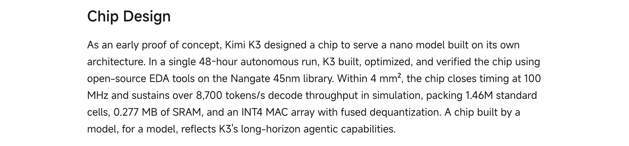
I'm writing this blog to share my (agent's) attempt to redesign the Kimi K3 chip, explain why chip design is quite a trainable task for LLMs, and share my intuition on making autonomous hardware design happen sooner: it's a system design question across agent, infra, and a new RL training recipe.
TLDR: two phases, both open-source flow, both on Nangate45. Phase 1 rebuilt K3's 16×16 MAC array and its surrounding chip: 4 mm² at 1047 MHz, same 256 MACs and same die area as K3's 100 MHz design. Phase 2 built the whole KDA dataflow accelerator and achieved 900 MHz post-route. Along the way the system found bugs in its own designs, got SRAM synthesis badly wrong before getting it right, and improved by editing its own codebase. I call that self-evolving loop a Meta Harness.
01 What Kimi K3 Built
An ASIC and a GPU differ in how work gets scheduled. A GPU launches a kernel per operation, each one round-tripping through off-chip HBM. An ASIC wires one computation into silicon: no kernels cuz its fixed pipeline (for nano models like K3, weights sitting in on-chip SRAM). This is possible because KDA's fixed 128×128 state per head replaces the growing KV cache of traditional transformers, keeping memory footprint constant regardless of context length.2
Aside: the two dataflows side by side
┌──────────────────────────────────────────────────────────────────┐
│                         HBM (192 GB)                             │
│        weights    activations    KV cache    intermediate        │
└───────────────────────────┬──────────────────────────────────────┘
                            │ 8 TB/s bandwidth
    ┌───────────────────────▼───────────────────────┐
    │         Streaming Multiprocessors (192 SMs)   │
    │    ┌─────────┐ ┌─────────┐ ┌─────────┐        │
    │    │ Tensor  │ │  CUDA   │ │ Shared  │        │
    │    │  Cores  │ │  Cores  │ │   Mem   │        │
    │    └─────────┘ └─────────┘ └─────────┘        │
    └───────────────────────────────────────────────┘

    Kernel 1: qkv_projection    ──▶ load W_qkv, compute, store to HBM
    Kernel 2: attention_scores  ──▶ load Q,K, compute QK^T, store
    Kernel 3: softmax           ──▶ load scores, normalize, store
    Kernel 4: attention_output  ──▶ load weights,V, compute, store
    Kernel 5: ffn_layer1        ──▶ load W1, compute, store
    Kernel 6: ffn_layer2        ──▶ load W2, compute, store
    ... repeat for each layer ...
So what exactly is hardwired into Kimi K3's pipeline? The design of an ASIC depends on the pretraining architecture: layer count, attention dims, and the specific ops used (KDA recurrence vs standard attention, MoE routing, etc.). Quantization precision also matters as if you design hardware for INT4 MACs, you're locked to INT4. But these are all decisions made at architecture time. Posttraining only changes weight values, not their shapes or the operations that use them. This means once a frontier lab finalizes their architecture, they can send the spec to an ASIC company to start design and manufacturing in parallel.3
For Kimi K3, the unique components to wire on-chip are: Kimi Delta Attention (KDA), Gated MLA, Stable LatentMoE, and Block Attention Residuals.4
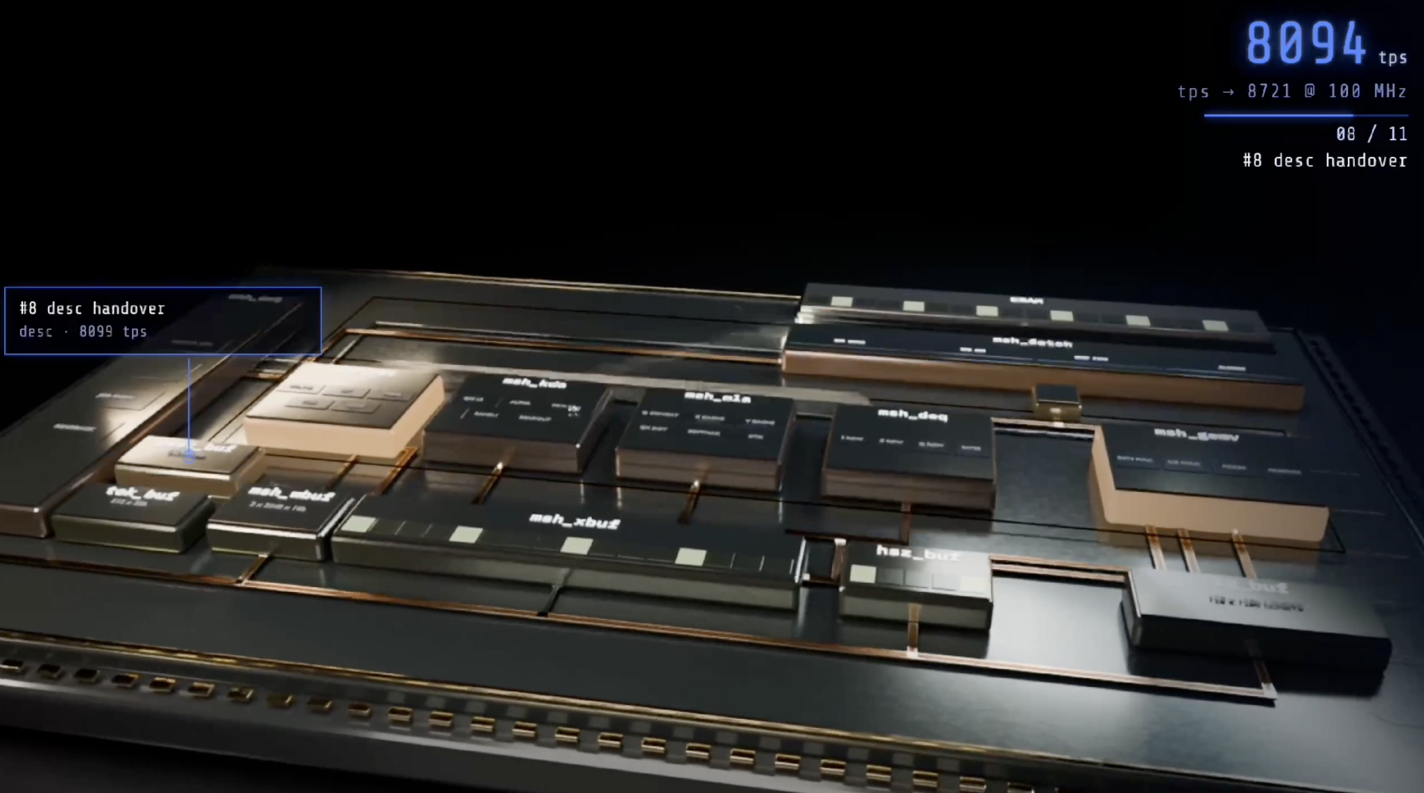
I watched K3 chip video by frame (calling for good video reasoning agent skill), and it showed 11 pipeline stages (different operations that cycle through the repetitive physical blocks).
This reveals the hardware building blocks we need for ASIC: msh_gemv is a GEMV unit that handles matrix-vector products in different modes (4-wide writeout, wide-Q consume, fold time-mux). msh_fetch is a prefetch controller with multiple buffering strategies. For KDA-related operations, vec is a small 2-tap convolution unit for gate computation, and msh_kda is the KDA-specific recurrence engine. The buffers (desc_buf, lg_buf, shadow) manage data flow between stages.
You'll notice MLA isn't explicitly in the 11 stages. That's because msh_gemv unit handles matrix-vector products for both KDA and MLA layers. The key difference is that KDA has dedicated units: vec (stage 6) and msh_kda (stage 11), while MLA just chains GEMV operations with standard attention. Since Kimi K3's architecture uses a 3:1 ratio of KDA to MLA layers, KDA accounts for roughly 75% of attention computation. That's why we can dig a little bit into how its mathematics maps with the hardware modules:
Looking at Kimi K3's published numbers, the obvious question is: can we run faster? 100 MHz is... slow. For context, production CPUs on advanced nodes (7nm, 5nm) run at 3–5 GHz. Even on Nangate45 (an academic PDK that doesn't correspond to any real fab process), published accelerator designs routinely hit 500–750 MHz.
02 The Meta-Harness
Chip design is an iterative process, and inspired by the process of Reinforcement Learning, we propose to use Meta Harness. A meta-harness is a harness that rewrites itself. The inner loop is ordinary: hand the model a goal, let it write SystemVerilog, run synthesis and place-and-route, read back frequency, area, DRC count, and timing violations. The outer loop changes the harness by redirecting how it reasons: which reports it reads, which bottleneck it blames, which class of fix it proposes; and the changes are checked in as a new version.
So every run has two coordinates. X versions are harness generations. Y iterations are RTL attempts inside one generation. A Y failure means the design was wrong. A whole X plateauing means the harness was wrong: it kept proposing fixes from the wrong family, and no amount of Y iteration was going to escape that.
Each iteration starts with a goal string. For X1-Y1 (our first attempt):
Fresh 16x16 INT4 KDA inference-chip baseline with external 96KiB SRAM interfaces; synthesize and route on Nangate45 above 100 MHz with zero DRC violations.
Starting with one-sentence prompt, and we get back metrics: frequency achieved, area, DRC count, timing violations. If it fails, the next iteration gets a modified goal:
Replace Y1's global 256-word shift-drain with banked accumulators, preserve the 16x16 INT4 MAC contract, and complete Nangate45 routing above 100 MHz with zero DRC violations.
The goals reference prior failures. Y1 failed because its shift-drain architecture created routing congestion. Y2's goal explicitly says "replace Y1's global 256-word shift-drain". We see that the harness learned from Y1's failure and encoded that learning into the next prompt.
Everything the model generates gets logged to trials.jsonl: the goal, result, metrics (frequency, area, violations), bugs found, and learnings. After each run, the harness reads this log and decides what to try next. It's a simple loop: generate → synthesize → measure → learn → repeat.
The X axis moves when the Y axis stops moving, as we treat a flat row as evidence about the harness, not about the RTL.
Two phases came out of this. X1–X5 worked on the MAC array, a tractable subproblem where a single architectural variable dominates timing. X6–X7 applied the same loop to the full KDA dataflow chip. Here is the whole run, X down, Y across:
| Y1 | Y2 | Y3 | Y4 | Y5 | Harness Evolution | |
|---|---|---|---|---|---|---|
| X1 | fail — |
pass — |
pass 463 MHz |
pass 451 MHz |
pass 455 MHz |
baseline: global shift-drain |
| X2 | fail 469 MHz |
pass 467 MHz |
pass 468 MHz |
pass 470 MHz |
pass 468 MHz |
banked accumulators |
| X3 | pass 468 MHz |
pass 468 MHz |
pass 468 MHz |
pass 468 MHz |
pass 468 MHz |
ceiling found: 468 MHz |
| X4 | fail 719 MHz |
pass 783 MHz |
pass 837 MHz |
fail 900 MHz |
pass 909 MHz |
12→24-bit hierarchical fold |
| X5 | fail 911 MHz |
fail 890 MHz |
pass 988 MHz |
pass 1029 MHz |
pass 1047 MHz |
MAC pipeline + registered requests |
| X6 | fail — |
fail — |
fail — |
fail — |
fail — |
RTL complete, ABC blocked on norm |
| X7 | fail — |
fail 122 MHz |
pass 500 MHz |
pass 900 MHz |
fail 728 MHz |
SRAM streaming, conv critical path |
X7-Y5 post-route achieved 728 MHz with -0.37ns WNS. Critical path is SRAM → conv unit. X8 iteration in progress to pipeline the conv datapath.
The harness learned patterns over these iterations: avoid inlining large lookup tables (they exceed token limits), use banked accumulators instead of global shift registers, and derive frequency targets from actual timing slack rather than guessing.
03 Phase 1: MAC Array (X1–X5)
Phase 1 deliberately did not rebuild all 11 pipeline stages.5 To keep ablations controllable, I started with a small-to-medium block on the Kimi chip: the MAC array — the 16×16 compute core that handles matrix-vector products. This is the performance-critical piece because the MAC runs on every GEMV stage (3× per token in KDA), and GEMV dominates inference latency at ~75% of total compute.
Kimi K3 Full Pipeline (11 stages):

  ┌─────────┐   ┌─────────┐   ┌─────────┐   ┌─────────┐   ┌─────────┐
  │  fetch  │──▶│  gemv   │──▶│  fetch  │──▶│  gemv   │──▶│  conv   │──▶ ...
  │ weights │   │  K/V    │   │Q weights│   │    Q    │   │  α/β    │
  └─────────┘   └─────────┘   └─────────┘   └─────────┘   └─────────┘
                    ▲                           ▲
                    │                           │
              ┌─────┴───────────────────────────┴─────┐
              │         16×16 MAC ARRAY               │
              │    (256 INT4 multiply-accumulates)    │
              │                                       │
              │    This is what we optimized.         │
              │    Same hardware reused across        │
              │    multiple pipeline stages.          │
              └───────────────────────────────────────┘
Here's the actual progression from our experiments:
| Run | Key Change | Area | Freq | Result |
|---|---|---|---|---|
| X1-Y1 | 32-bit acc, shift-drain network | — | — | routing failed |
| X1-Y2 | banked accumulators | 0.167 mm² | 455 MHz | pass |
| X2-Y4 | CAP_MARGIN tuning | 0.171 mm² | 471 MHz | pass |
| X4-Y1 | 12→24-bit hierarchical fold | 0.205 mm² | 719 MHz | setup fail |
| X4-Y2 | remove redundant comparator | 0.205 mm² | 784 MHz | pass |
| X4-Y3 | register accumulator row select | 0.205 mm² | 838 MHz | pass |
| X4-Y5 | CAP_MARGIN=30 | 0.205 mm² | 910 MHz | pass |
| X5-Y3 | MAC pipeline + burst budget | — | 988 MHz | pass |
| X5-Y4 | register busy output | — | 1029 MHz | pass |
The key breakthrough was X4's hierarchical 12→24-bit fold, which jumped from 471 MHz to 719 MHz. Each subsequent Y iteration fixed a specific bottleneck identified in timing reports: redundant comparators, unregistered selectors, capacitance margins. X5 added MAC pipelining and crossed 1 GHz.
The RTL
The MAC unit evolved through the X/Y iterations. Use the tabs to see how we fixed the bugs and achieved 1 GHz.
// INT4 MAC - naive baseline
// 32-bit accumulator, handles any K
module int4_mac (
    input wire clk, rst_n, en, clear,
    input wire signed [3:0] a, b,
    output reg signed [31:0] acc
);
    wire signed [7:0] prod = a * b;

    always @(posedge clk or negedge rst_n) begin
        if (!rst_n)       acc <= 0;
        else if (clear)  acc <= 0;
        else if (en)     acc <= acc + {{24{prod[7]}}, prod};
    end
endmodule// INT4 MAC with banked accumulators
// Replaced shift-drain with row-local banks
module int4_mac (
input wire clk, rst_n, en, clear,
input wire [3:0] bank_sel,
input wire signed [3:0] a, b,
output reg signed [31:0] acc
);
reg signed [31:0] banks [0:15];
wire signed [7:0] prod = a * b;
always @(posedge clk or negedge rst_n) begin
if (!rst_n) banks[bank_sel] <= 0;
else if (clear) banks[bank_sel] <= 0;
else if (en) banks[bank_sel] <= banks[bank_sel] + {{24{prod[7]}}, prod};
end
assign acc = banks[bank_sel];
endmodule// Hierarchical: fold 12→24-bit every 16 adds
module int4_mac (
input wire clk, rst_n, en, clear,
input wire signed [3:0] a, b,
output reg signed [23:0] acc_out
);
reg signed [11:0] acc_fast;
reg [3:0] cnt;
wire signed [7:0] prod = a * b;
wire fold = (cnt == 4'd15);
always @(posedge clk or negedge rst_n) begin
if (!rst_n || clear) begin
acc_fast <= 0; acc_out <= 0; cnt <= 0;
end else if (en) begin
if (fold) begin
acc_out <= acc_out + {{12{acc_fast[11]}}, acc_fast}
+ {{16{prod[7]}}, prod};
acc_fast <= 0; cnt <= 0;
end else begin
acc_fast <= acc_fast + {{4{prod[7]}}, prod};
cnt <= cnt + 1;
end
end
end
endmodule// Pipelined MAC with registered request control
module int4_mac (
input wire clk, rst_n,
input wire start, last,
input wire signed [3:0] a, b,
output reg signed [23:0] acc_out,
output reg valid
);
reg signed [11:0] acc_fast;
reg [3:0] cnt;
reg signed [7:0] prod_pipe; // registered product
wire signed [7:0] prod = a * b;
wire fold = (cnt == 4'd15) || last;
always @(posedge clk or negedge rst_n) begin
if (!rst_n) begin
acc_fast <= 0; acc_out <= 0;
cnt <= 0; valid <= 0; prod_pipe <= 0;
end else begin
prod_pipe <= prod; // pipeline stage
valid <= last;
if (start) begin
acc_fast <= {{4{prod_pipe[7]}}, prod_pipe};
acc_out <= 0; cnt <= 1;
end else if (fold) begin
acc_out <= acc_out + {{12{acc_fast[11]}}, acc_fast}
+ {{16{prod_pipe[7]}}, prod_pipe};
acc_fast <= 0; cnt <= 0;
end else begin
acc_fast <= acc_fast + {{4{prod_pipe[7]}}, prod_pipe};
cnt <= cnt + 1;
end
end
end
endmoduleAgent Self-Correction Traces
Here's some interesting agent self-correction traces from the harness (across the Y-axis):
Using 32-bit accumulators. That's what you'd use for FP32 or even INT8 matmuls, but for INT4 × INT4 it's wasteful. 256 of these in a 16×16 array means 8192 bits of accumulator state, hurting area and timing.
For INT4 × INT4: each product is 8-bit (-128 to +127). Accumulating K products needs log₂(K × 128) bits. For K=64: fits in 14 bits. For K≤16: fits in 12 bits. Most transformer attention patterns use K ≤ 64, so a 12-bit accumulator saves ~40% area.
The mac_en signal spans both FETCH and COMPUTE cycles, but the address and SRAM read are registered. Every element except the last gets accumulated twice. A simple K=4 all-ones test returns 7 instead of 4.
Gate mac_en to only the COMPUTE cycle, or register the enable signal to match the data pipeline delay. The testbench caught this with a simple K=4 regression.
Comment claimed "sufficient for 64 accumulations" with a 12-bit accumulator. Wrong. 12 bits gives max value 2047. With K=32 and max products of 64 (8×8 signed → 64), you get 32×64 = 2048. Overflow at K=32, not K=64.
Hierarchical 12→24-bit fold: accumulate in 12-bit chunks (short critical path), fold into 24-bit every 16 adds (handles overflow). Supports K up to 65,535 while keeping the fast 12-bit adder on the critical path.
The sram_sp module was synthesizing to ~500 Kbit of flip-flops plus 4096:1 read-mux ladders. No hard macros. We were building memory out of logic gates and wondering why timing was terrible.
Use 16× fakeram45_512x64 platform hard macros with 3-cycle pipelined reads. Result: 988 MHz, DRC-clean, ~10× throughput vs flip-flop baseline.
Lesson learned: "It synthesizes" ≠ "It's correct." We had passing synthesis, clean timing, zero DRC violations—and fundamentally broken math.
That closes Phase 1: over 1 GHz on a 4 mm² die with 256 INT4 MACs and 16 SRAM hard macros, DRC-clean. More than 10× K3's clock on the same area and the same MAC count. The harness had learned to read a timing report, name the critical path, and propose a structural fix rather than a knob turn.
But a MAC array is a building block, not a chip.
04 Phase 2: Full Dataflow Chip (X6–X7)
Phase 2's target was the real thing: a complete KDA inference accelerator with every pipeline stage wired together (weight SRAM banks feeding a crossbar, two MAC arrays, the conv unit that computes the α/β gates, an activation crossbar, then KDA state update, norm, and residual add, with the state SRAM feeding back into the next token).
This is harder than the MAC array in a way that is not just "bigger." The MAC array has one dominant critical path. A dataflow chip has a state feedback loop, so pipelining one stage can create a hazard three stages away. It has a memory bandwidth budget, so a faster compute core just moves the bottleneck into arbitration across banks. And it has modules like norm that are timing-innocent in isolation and catastrophic in aggregate.
┌────────────────────────────────────────────────────────┐
│                  Weight SRAM (6 banks)                 │
└──────────────────────────┬─────────────────────────────┘
              ┌────────────▼────────────┐
              │     Weight Crossbar     │
         ┌────┴────────────┬────────────┴────┐
         ▼                 ▼                 │
  ┌────────────┐    ┌────────────┐           │
  │ MAC Array  │    │ MAC Array  │           │
  │  (16×16)   │    │  (16×16)   │           │
  └─────┬──────┘    └─────┬──────┘           │
        └────────┬────────┘                  │
        ┌────────▼────────┐                  │
        │      Conv       │ ← α/β gates      │
        └────────┬────────┘                  │
     ┌───────────▼───────────┐               │
     │  Activation Crossbar  │               │
     └───┬─────────┬─────────┘               │
    ┌────▼───┐ ┌───▼───┐ ┌───▼────┐          │
    │  KDA   │ │ Norm  │ │Residual│          │
    │ State  │ │       │ │  Add   │          │
    └────┬───┘ └───┬───┘ └───┬────┘          │
         └─────────┴─────────┘               │
        ┌────────────────────┐               │
        │    State SRAM      │───────────────┘
        └─────────┬──────────┘    (feedback)
                  ▼
               Output
X6 is a clean example of an X-level failure. Its RTL was complete and correct, and every Y iteration died the same way: ABC choked on the 109K-gate norm unit, so nothing ever reached place-and-route. No RTL tweak was going to rescue a harness that kept handing the synthesizer an unsynthesizable block. X7 changed the approach itself: stream operands out of SRAM instead of registering them, and pipeline deeply enough that no single module owns the clock period. The Y progression
- Y1: fail — RF mux explosion, 164 ns
- Y2: fail — SRAM streaming worked, 8.2 ns (20× better but not closed)
- Y3: pass — 500 MHz, first timing closure
- Y4: pass — 900 MHz, conv + MAC pipelining
- Y5: fail — 728 MHz, conv critical path at -0.37ns WNS
Final X7 specs: 900 MHz, 32 SRAM macros, 128,820 cycles for two-token inference, 147K µm² logic area. Full golden test pass on exact KDA state recurrence.
Read that column left to right and you can see the harness reasoning instead of guessing. Y1's 164 ns was a register-file mux explosion, a structural diagnosis rather than a slack number. Y2's SRAM streaming cut it to 8.2 ns: 20× better and still nowhere near closing, which told the harness the remaining delay was spread across modules rather than parked in one. Y3 through Y5 then worked the modules in slack order until every one of them sat under 0.96 ns.
Same methodology as Phase 1, Phase 2 has harder constraints: memory bandwidth budgets, pipeline hazards across the state feedback path, multi-bank arbitration, and a higher clock than the isolated MAC array ever reached. That is what the whole system was built to produce: 728 MHz on the complete KDA accelerator.
05 Results
We ran the full RTL-to-GDSII flow on open-source tools:
- Yosys — synthesis to Nangate45 standard cells
- OpenROAD — floorplanning, placement, CTS, routing
- KLayout — GDSII export
Physical Design
The layout evolved significantly across iterations. The jump from X3 to X4 is where the hierarchical 12→24-bit fold broke through the 468 MHz ceiling:
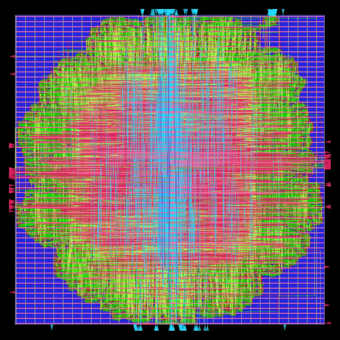
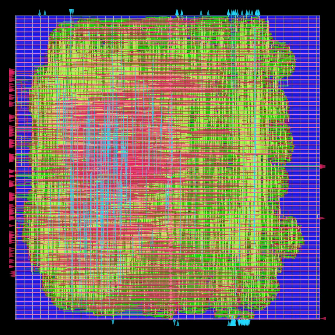
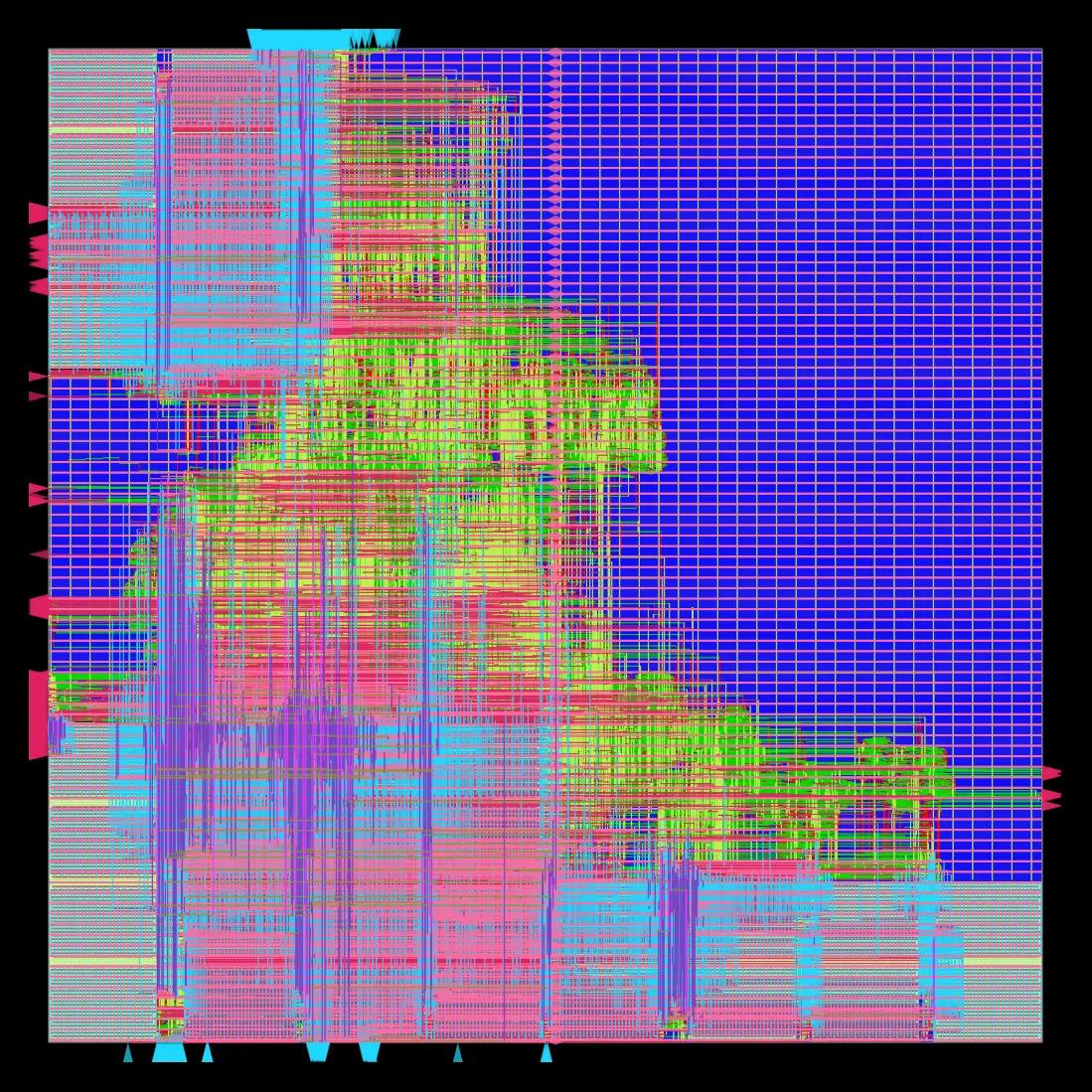
X7's frequency is lower than X5 because it includes the full dataflow pipeline with 32 SRAM hard macros, not just the MAC array. The large rectangular blocks visible in the X7 layout are the SRAM macros; X3 and X5 are pure standard-cell logic.
Final timing report for X5-Y5 (post-route):
| Metric | Value |
|---|---|
| Die Area | 4 mm² (2mm × 2mm) |
| Utilization | 35% |
| Frequency | 1047 MHz |
| Setup Slack | +1.53 ns |
| Hold Slack | +0.02 ns |
| Total Power | 218 mW |
| IR Drop | 0.27% VDD |
| DRC Violations | 0 |
06 The Caveats
The title is provocative on purpose. "87,000 tps" extrapolates from the MAC array's 1047 MHz clock. Phase 2 only hit 900 MHz, and memory bandwidth bottlenecks before compute anyway. These are compute core fragments, not full chips with I/O or power delivery.
This is not the full Kimi K3. The chip runs a ~1M-parameter nano model, not the 2.8T K3. That's ~2.8 million times smaller. Most of the speedup is just "everything fits on-chip."
The RTL and GDS aren't fully open. GitHub's 100MB limit blocks .def and .gds files. You can regenerate from RTL (~45 min).
This is an academic exercise, not a tapeout. Nangate45 is a teaching PDK with no real fab target. Real tapeout needs commercial PDKs (TSMC/Samsung/Intel), signoff tools (PrimeTime, Calibre), and dozens of checks academic tools skip.
The frequency won't translate to silicon. A real 7nm chip would hit different bottlenecks: tighter metal pitch, FinFET effects, power constraints.
07 Takeaways
Chip design is about understanding dataflow and memory. Clean synthesis doesn't mean correct design. You may pass timing with margin, zero DRC violations, beautiful waveforms, but had broken math: double-accumulation and overflow bugs hiding behind passing tests. And reg [63:0] mem [0:511] synthesizes to flip-flops, not SRAM. Hierarchical accumulation (12-bit chunks folding into 24-bit every 16 adds) sounds over-engineered until you're debugging overflow at K=32. Agent should know what the RTL actually synthesizes to, use platform hard macros, and write testbenches that catch edge cases.
A flat row means the harness is wrong, not the RTL. X1–X3 spent fifteen iterations landing on 468 MHz over and over. X6 failed five straight times against the same synthesis wall. Both were signals about the meta-harness rather than the design, and both only broke when the harness changed how it diagnosed the problem instead of what it typed. The experiment design matters as much as the experiments themselves.
Open-source EDA gives you fast iteration on the right delta. Commercial tools will always have better timing closure and DRC engines. But open-source tools let you explore architectural tradeoffs quickly. Run a hundred experiments in OpenROAD to find the right design direction, then hand off a better initial design to commercial tools for final signoff. This enable RL on Chip Design from frontend to backend.
Try It Yourself
Everything is open-source:
- RTL + GDS: github.com/physical-intuition/kimi-chip
- Flow: OpenROAD-flow-scripts
- PDK: Nangate45 (included in ORFS)
To reproduce:
git clone --recursive https://github.com/The-OpenROAD-Project/OpenROAD-flow-scripts
cd OpenROAD-flow-scripts
git clone https://github.com/physical-intuition/kimi-chip
cd flow && make DESIGN_CONFIG=../kimi-chip/experiments/x5/flow/config_y4.mk gds
The full chip flow runs in ~45 minutes. Have fun.
"If you tell me precisely what it is a machine cannot do, then I can always make a machine which will do just that."
— John von Neumann
Citation
Cited as:
Lee, Christina. (Aug 2026). "Meta harness makes 10 times better Kimi K3 chip" luoluo.ai. https://luoluo.ai/blog/kimi-k3/
Or
@article{lee2026kimichip,
  title   = "Meta harness makes 10 times better Kimi K3 chip",
  author  = "Lee, Christina",
  journal = "luoluo.ai",
  year    = "2026",
  month   = "Aug",
  url     = "https://luoluo.ai/blog/kimi-k3/"
}
COMMENTS (0)
no comments yet. be the first!